Overcoming strict GPU memory limits unlocks massive enterprise AI scaling.
How JEDEC standards and HBM4 memory bandwidth specs resolve critical AI chip bottlenecks in cloud infrastructure.
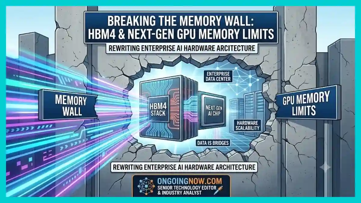
Modern enterprise AI hardware architecture is undergoing a foundational shift as hardware scalability for AI models encounters rigid physics limitations. To sustain complex LLM training hardware requirements, cloud infrastructure hardware optimization must now transition away from raw compute scaling and focus entirely on overcoming AI chip memory bottlenecks. High bandwidth memory AI servers represent the critical vector for this evolution, as next-gen GPU memory limits dictate the economic viability of training and deploying frontier models. The industry adoption of processing unit memory standards like HBM4 addresses these exact constraints by rewriting how memory stacks interface with processing silicon.
The technological transition involves deep collaboration across global standards bodies, semiconductor foundries, and cloud providers. The Joint Electron Device Engineering Council (JEDEC) has accelerated the formalization of HBM4 memory bandwidth specs to standardize a 2048-bit wide memory interface, a massive structural leap over the 1024-bit interface used in HBM3 and HBM3E. Foundries like Taiwan Semiconductor Manufacturing Company (TSMC) and memory pioneers including SK Hynix, Samsung Electronics, and Micron are retooling fabrication lines to support advanced packaging methods, such as chip-on-wafer-on-substrate (CoWoS), to integrate these ultra-wide memory stacks. Meanwhile, enterprise data center chip trends show hyperscalers like Amazon Web Services (AWS), Microsoft Azure, and Google Cloud configuring infrastructure around these tighter physical footprints to manage escalating thermal and power densities.
The Core Physics Driving Next-Gen GPU Memory Limits
The core challenge in contemporary AI hardware design is the “memory wall”—the widening performance gap between how fast a processor can execute mathematical instructions and how fast it can read data from memory. While floating-point operations per second (FLOPS) have scaled dramatically over the last decade, memory access times and power efficiency have lagged. In large language model applications, particularly during the auto-regressive generation phase, the processor must load billions of weights from memory into its local registers for every single token generated. If the memory subsystem cannot deliver those weights fast enough, the expensive execution units sit idle, executing a phenomenon known as memory-starved underutilization.
+-------------------------------------------------------------------+
|                     THE ENTERPRISE MEMORY WALL                    |
+-------------------------------------------------------------------+
|  Compute Capability (FLOPS)   | Scaled exponentially (e.g., ~10x) |
|  Memory Bandwidth (GB/s)      | Scaled linearly (e.g., ~2.5x)     |
+-------------------------------------------------------------------+
|  Result: Processors spend critical clock cycles waiting for data  |
+-------------------------------------------------------------------+
To counter this bottleneck, processing unit memory standards are transitioning to HBM4, which modifies the physical interface. Unlike conventional memory that connects via trace lines on a printed circuit board, high bandwidth memory stacks vertically directly onto the processor’s silicon interposer. HBM4 doubles the interface width to 2048 bits. This structural modification allows data to move across thousands of microbumps simultaneously, drastically lowering the energy required per bit transferred while multiplying the aggregate data volume that can reach the logic units.
Technical Specifications and HBM4 Memory Bandwidth Specs
The engineering shift from HBM3E to HBM4 marks the first time high bandwidth memory abandons traditional memory controller logic interfaces in favor of advanced foundry logic processes. In earlier generations, the base die at the bottom of the memory stack was fabricated using standard DRAM manufacturing nodes. HBM4 utilizes advanced foundry sub-wavelength nodes (such as 4nm or 5nm classes) for the base layer, enabling the integration of complex test routing and direct vertical interconnects.
This structural upgrade enables data transfer rates exceeding 1.5 terabytes per second ($TB/s$) per stack. When grouped in typical configurations of six to eight stacks around a central processor, an enterprise AI chip can access between $9.0\text{ }TB/s$ and $12.0\text{ }TB/s$ of aggregate local bandwidth. This throughput is mandatory for sustaining the high-density matrix math operations required by modern transformer blocks without stalling execution pipelines.
       HBM3E Architecture (1024-bit)           HBM4 Architecture (2048-bit)
    +---------------------------------+     +---------------------------------+
    |        DRAM Layers (x8/x16)     |     |       DRAM Layers (x12/x16)     |
    +---------------------------------+     +---------------------------------+
    |   Standard DRAM Base Die Layer  |     |   Advanced Logic Base Die Layer |
    +---------------------------------+     +---------------------------------+
    |========= 1024-bit Bus ==========|     |======= 2048-bit Wide Bus =======|
The vertical stacking capability expands to support 12-layer and 16-layer DRAM configurations, pushing per-stack physical capacity to 48 gigabytes ($GB$) or 64 $GB$. For an integrated server node utilizing next-gen GPU memory limits, this delivers up to 512 $GB$ of ultra-fast co-packaged memory per accelerator socket, transforming how large datasets are managed locally on-chip.
Architectural Benchmarks and Training Hardware Realities
Quantifying the impact of memory subsystems requires evaluating hardware scalability for AI models under real-world compute profiles. LLM training hardware requirements are split into two core operational regimes: compute-bound workloads, such as dense matrix multiplication during the forward pass, and memory-bandwidth-bound workloads, which dominate activation caching, layer normalization, and attention calculations.
As models scale beyond hundreds of billions of parameters, distributed training frameworks rely heavily on tensor parallelism, where individual layers are sliced across multiple accelerators. The performance of these configurations is heavily gated by interconnect and memory capacity constraints.
| Metric / Specification Parameter | HBM3E Standard Target | HBM4 Advanced Specification |
| Interface Bus Width (Per Stack) | 1024 bits | 2048 bits |
| Maximum Data Transfer Rate per Pin | ~9.6 Gbps | ~12.0 – 14.0 Gbps |
| Peak Aggregate Bandwidth (6 Stacks) | ~7.0 TB/s | ~10.5 – 12.6 TB/s |
| Typical Physical Stack Layering | 8-layer / 12-layer | 12-layer / 16-layer |
| Maximum Density per Base Die Assembly | 288 GB | Up to 512 GB |
| Base Interconnect Die Technology | Conventional DRAM | Advanced Foundry Logic (4nm/5nm) |
Analysis Component: The technical shift to a 2048-bit bus width means that even at identical clock frequencies, HBM4 delivers twice the theoretical throughput of HBM3E. This permits system designers to lower operational voltages, directly addressing the strict thermal design power (TDP) thresholds of modern enterprise data centers.
Implementation Strategies for Cloud Infrastructure Optimization
Deploying high bandwidth memory AI servers into hyperscale environments introduces significant engineering complexities. Cloud infrastructure hardware optimization requires balancing power, structural packaging precision, and systematic cooling architectures to prevent localized thermal throttling.
Advanced Packaging Dependencies: Integrating a 2048-bit wide memory bus requires transitioning from traditional interposers to advanced silicon and organic substrate systems. Foundries use fine-pitch microbump technologies to align the tens of thousands of connections between the logic die and the HBM4 stacks.
Thermal Management Realities: Concentrating up to 512 $GB$ of high-density memory directly adjacent to a high-power logic die creates massive heat generation within a compact space. Enterprise data center chip trends show an accelerated departure from air cooling toward direct-to-chip liquid cooling loops capable of dissipating over 1,000 watts per socket.
Interconnect Power Allocations: As local memory capacity grows, data must flow seamlessly across nodes. System architectures allocate considerable energy envelopes to high-speed chiplet-to-chiplet buses, ensuring that off-chip communication links do not invalidate the performance gains achieved by on-chip memory upgrades.
Operational Reliability and Technical Vulnerabilities
The consolidation of high-performance logic and multi-layered memory stacks onto a single package introduces unique reliability, availability, and serviceability (RAS) liabilities. With billions of microbumps operating within tight physical proximity, thermal cycles can trigger structural microscopic fractures or electrical cross-talk, resulting in intermittent data corruption or complete device failure.
To maintain uptime across thousand-node clusters, processing unit memory standards incorporate advanced on-die Error-Correcting Code (ECC) algorithms alongside real-time link-layer retry mechanisms. These safety layers detect and repair single-bit faults dynamically. However, multi-bit failures or permanent physical degradation within an HBM4 stack can require replacing the entire multi-thousand-dollar processing module, since the memory is permanently bonded to the logic unit. Furthermore, malicious physical side-channel vectors, such as localized fault injection attempts exploiting thermal fluctuations, remain an active area of evaluation for infrastructure security architects.
Market Outlook and Data Center Evolution
Enterprise data center chip trends indicate that memory configuration is now the primary factor determining capital expenditure efficiency in AI infrastructure. Organizations are evaluating total cost of ownership (TCO) not by the raw volume of accelerators deployed, but by the utilization efficiency of those accelerators.
+-------------------------------------------------------------------+
|               ENTERPRISE DATA CENTER HARDWARE TCO                 |
+-------------------------------------------------------------------+
|  Old Paradigm: Evaluate raw accelerator count & peak FLOPS.       |
|  New Paradigm: Optimize effective throughput per Watt & dollar.  |
+-------------------------------------------------------------------+
|  Result: HBM4 investments lower idle time, maximizing returns.     |
+-------------------------------------------------------------------+
By mitigating AI chip memory bottlenecks, next-generation memory architectures allow large clusters to complete training runs with fewer node communication steps, directly optimizing power usage effectiveness (PUE) metrics. As model architectures diversify into mixture-of-experts (MoE) topologies—which require massive memory footprints but sparse activation pathways—high-capacity, high-bandwidth local memory systems will dictate which data centers can run frontier enterprise workloads efficiently.
Expert Insights and Technical Commentary
Industry specialists emphasize that the transition to next-gen GPU memory limits represents a structural shift in hardware engineering. The physical and economic constraints of traditional scaling methods have forced silicon designers to re-engineer how components communicate at the micro-architectural level.
Dr. Kim Hyoung-Seon, a leading senior research fellow in semiconductor integration, notes:
“Doubling the interface width to 2048 bits removes the structural scaling limitations that hampered previous iterations. By moving the base layer of HBM4 to advanced logic nodes, we are no longer just building a passive memory buffer; we are building an intelligent data routing network directly alongside the host processor.”
Addressing the logistical challenges of fabricating these components, TSMC Advanced Packaging Engineer Lin Wei-Chung states:
“The alignment tolerances required for CoWoS integration with 2048-bit routing demand placement accuracy measured in single-digit microns. The thermal expansion profiles of the memory base logic must be perfectly synchronized with the central computing die to avoid physical delamination during prolonged workloads.”
Analyzing the broader infrastructure impacts, Enterprise Infrastructure Analyst Sarah Jenkins explains:
“Hyperscale cloud optimization is no longer determined solely by the speed of the tensor cores. If your memory channels are starved, your infrastructure efficiency plummets. HBM4 is an absolute requirement for cloud operators to maintain sustainable margins as enterprise AI models scale into multi-trillion parameter territories.”
Evaluating data center operations, Uptime Institute Systems Engineer Marcus Vance comments:
“The real bottleneck in modern facilities is power and heat density. Bringing high bandwidth memory architectures online requires a parallel overhaul of data center cooling topologies, shifting from raised-floor air systems to closed-loop liquid networks.”
Stay sharp with Ongoing Now!
Source and Data Limitations: This technical brief is synthesized from published specifications by the Joint Electron Device Engineering Council (JEDEC), technical releases from semiconductor foundries (TSMC), and verified whitepapers from major memory manufacturers (SK Hynix, Samsung, Micron). Data is bounded by confirmed 2025/2026 industry architectural standards and excludes unverified vendor marketing projections or experimental laboratory prototypes lacking formal standardization timelines. Performance metrics assume optimized workloads and do not account for variable software framework inefficiencies.